
 July 21, 2026
Plasma surface treatment in chip manufacturing – selective, inline, and cycle-time optimized
Semiconductors are in short supply right now and demand is showing no signs of easing off. With this in mind, increasing throughput is just as important as increasing yield to deliver a high quality product. In its capacity as a long-standing and experienced supplier, the technology leader Plasmatreat GmbH from Steinhagen, Germany, has therefore faced up to the increased challenges and developed a fully automated inline system for selective pretreatment with Openair-Plasma that is designed according to market requirements. In doing so, customers benefit from a flexible, potential-free, high-speed treatment.
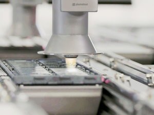
Vacuum plasma has been used for many applications in the semiconductor industry over the years. The Openair-Plasma process from Plasmatreat, on the other hand, facilitates a fast, inline process for pretreatment under atmospheric conditions that is suitable for surface treatments such as microfine cleaning, activation, and plasma coating. This technology can be used in a variety of ways in the field of semiconductor manufacturing – for example, it enables microfine cleaning in the packaging processes, thereby replacing the vacuum chamber in the production of chip packaging in an efficient and cost-effective manner. Other areas of application include wire and die bonding, thermal compress bonding, and pre-molding.
The PTU (Plasma Treatment Unit), which is designed for the specific process engineering sequence of semiconductor manufacturing, can be seamlessly integrated into production lines. It offers various kinematics and automation options, such as precise-fit handling of assemblies and components, and allows efficient surface treatment.
Plasmatreat developed the dual-lane concept specifically for high-speed treatment of up to 1.5 m/s. The dual-lane-concept is essentially suitable for various applications, with the system designed for both JEDEC trays and lead frames. It has different processing concepts according to the cycle time, and communication within the production line takes place via the standard equipment interface protocol interface in the semiconductor industry, SECS/GEM.
More info in the original Press Release.
