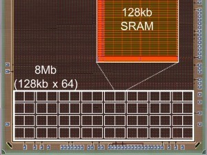
New Embedded SRAM with Industry's Lowest Standby Power

Renesas Electronics announced the successful development of a new low-power SRAM circuit technology that can be embedded in application specific standard products (ASSPs) for Internet of Things, home electronics, and healthcare applications. The new technology provides a function for switching dynamically with low power overhead between active operation in which the CPU core performs read and write operations of the embedded SRAM, and the standby mode in which the stored data is retained.
Renesas applied its in-house 65 nm node silicon on thin BOX (SOTB) process for the prototype development of the embedded SRAM. The prototype SRAM achieves simultaneous high-speed readout time of 1.8 ns during active operation, and ultra-low power consumption of 13.7 nW/Mbit in standby mode. The SRAM takes advantage of the SOTB structure by using dynamic substrate back bias control to achieve the industry's lowest standby-mode power consumption, which is only one-thousandth of the power consumption during normal standby mode (more info).


