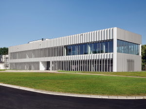
Plasmatreat opens new technology and research center

Plasmatreat opens its new technology and research center, Plasma Campus, at the company’s headquarter in Steinhagen in October 2019. In the 1400 square meter facility new areas of application for plasma technology will be developed. In addition, the new building accommodates seminar and conference rooms for approx. 200 participants as well as rooms for machine acceptance tests and customer trainings.
The Technology and Research Centre has various divisions which focus on the development of plasma solutions for a wide variety of applications. The center’s staff will not only work on processes related to plasma coatings, also Openair-Plasma technology for electronics production will be developt continuously.
"Open-air plasma technology offers a multitude of applications for electronics production. It ranges from the surface cleaning of leadframes to micro-cleaning of contact surfaces of bond pads prior to wire bonding. Even in printed circuit board production oxidation layers can be removed from copper surfaces using plasma. Openair-Plasma is also used in the actual component production, for example for cleaning printed circuit board prior to conformal coating. Or to ensure a strong bond between various materials through plasma activation before casting for final device construction. These are just some of the areas of application in electronics production," states Christian Buske, Managing Director of Plasmatreat GmbH.
These are standard applications that have been used in electronics production for more than 20 years. "Our goal is to establish Openair-Plasma as a reproducible, effective, environmentally friendly and resource-saving process also for small and medium-sized production. Therefore, we will use the new premises for training and further education in plasma technology," says Buske. However, Buske knows that in addition to standard applications, many other applications are still untouched. Machine manufacturers, for example, are considering the integration of Openair-Plasma technology in production systems. "This is precisely why we have built our new technology and research center. We want to intensify our work with our customers on new solutions and areas of application, because the increasing packing density on printed circuit boards and the associated miniaturization require to rethinking surface treatment," says Buske. The new building will be officially opened on October 30.


