
 October 21, 2026
 Professional magazine and portal dedicated to electronics
 SY757xx: Microchip’s LVCMOS Clock Buffers Link Latest CPUs with Higher Voltage Components
Author: Jan Robenek
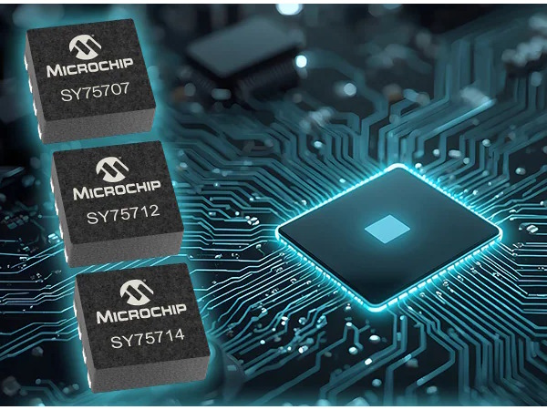
The demand for low-voltage clock drivers continues to grow with the rapid adoption of advanced FinFET process nodes used in high-performance FPGAs, SoCs, AI accelerators and next-generation CPUs. Printed circuit board designers face increasing challenges due to the limited availability of standard 1.2V LVCMOS clock buffers and level-translating buffers capable of converting higher-voltage clock signals to the lower-voltage levels required by these advanced devices. Conventional approaches that rely on discrete components and voltage-divider techniques can compromise signal integrity and clock duty-cycle accuracy while increasing board complexity and component count.
Microchip Technology has introduced the SY757xx family, a comprehensive portfolio of 1.2V-output LVCMOS clock buffers, designed to address these challenges. The new devices simplify system design by eliminating the need for traditional discrete-component implementations while delivering ultra-low additive jitter performance. To provide flexibility for supporting legacy board power supplies and different clock-source voltage levels, the devices support a broad range of supply voltage (VDD) and a wide operating frequency range. The SY757xx family enables ultra-low additive jitter clock distribution while maintaining the high clock resolution and signal integrity required for today’s high-speed FPGA, SoC and CPU platforms.
Microchip’s SY757xx family strengthens the clock buffer’s role as a critically important SoC and FPGA interface for clock distribution and clock fanout functionality in application platforms where signal integrity is paramount. These platforms demand high-speed parallel processing, hardware reconfigurability, low latency and efficient real-time computing. These capabilities are required for applications ranging from embedded vision and video processing to AI/ML acceleration, industrial control and IoT, networking and communications, and signal processing and embedded systems.
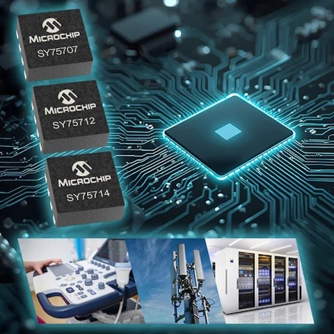
Additive Jitter: 16.9 fs
Launching three products in production and eight that are sampling in limited volumes, the family spans a wide array of configurations in three space-saving packaging options. The devices protect against clock distortion across a 0 Hz to 250 MHz frequency spectrum while also offering a broad range of power supply input and output options across the 1.2V to 3.3V voltage-translation input range. This includes a single-chip option that reliably interconnects 3.3V components to FPGAs and SoCs with a 1.2V clock signal requirement. Additive jitter is as low as 32 femtoseconds and 16.9 fs, respectively.
Pricing and Availability
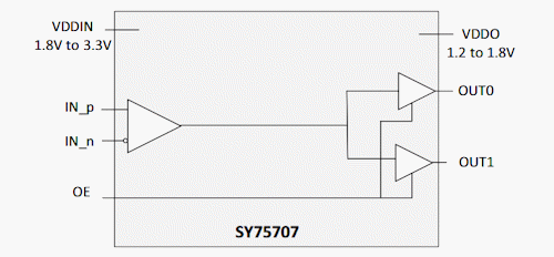
The low-power LVCMOS clock buffer family’s SY75707TWL-TR, SY75712TWL-TR and SY75714TWL-TR devices are in volume production. The SY75707TWL-TR supports differential input to two LVCMOS output and is housed in an 8-pin Very-thin Dual Flat No-lead (VDFN) package. The SY75712TWL-TR and SY75714TWL-TR devices enable either 2 or 4 LVCMOS outputs operating at 1.2V to 1.8V rail, respectively, and are housed in 8-pin Thin Dual Flat No-lead (TDFN) packages. They are priced from $0.50 to $0.83 per unit depending on configuration, in volumes of 10,000.
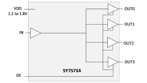
The other eight SY757xx family members bridge to 1.2V-to-1.8V LVCMOS outputs from a choice of single-ended 1.2V to 3.3V LVCMOS inputs, single-ended 1.2V to 1.8V LVCMOS inputs, or differential 1.8V to 3.3V inputs. There are also options for an output-enabled (OE) fanout buffer. All the sampling devices are housed in 8-pin VDFN packages.
Related Links
[1] Press release, https://www.microchip.com/en-us/about/news-releases/products/microchip-clock-buffers-link-latest-socs-and-fpgas-with-higher-voltage-components
[2] 1.2V, Ultra-Low Additive Jitter LVCMOS Buffers, https://www.microchip.com/en-us/products/clock-and-timing/components/clock-data-distribution/buffers/low-voltage-buffers
robenek@dps-az.cz
